Learn About the Display
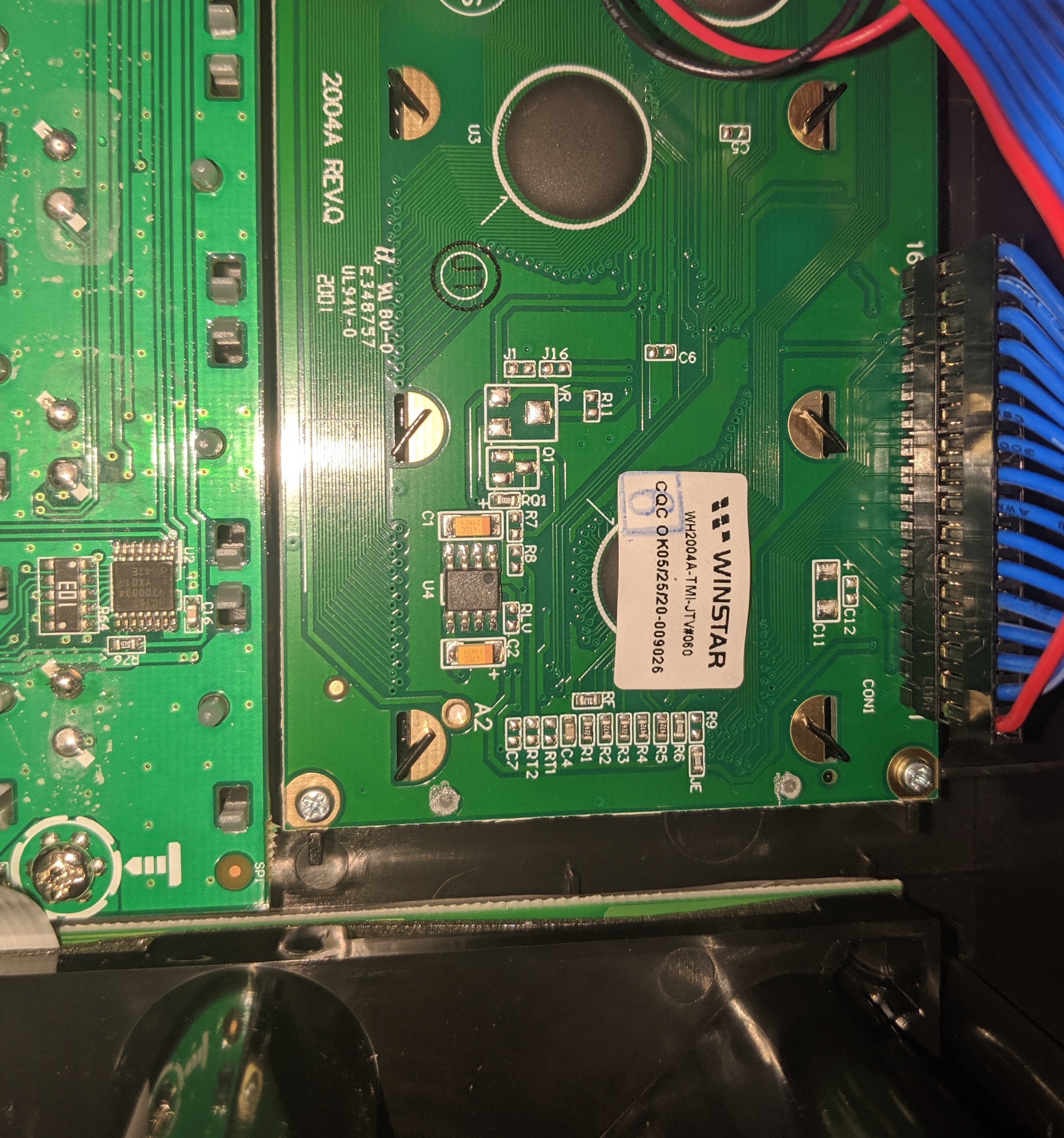
The LCD Display on the MPK249 is a Winstar model number
WH2004a.
Here is the full specification distributed by the manufacturer.
There are a couple of different ways to drive it, but our brand uses ‘6800 interface (ST7066 IC)’. We’re going to have to
initialize it, send some clock pulses to it from our STM32, and come up with a loop to update the screen.
[Here is the data sheet for the ST7066] (https://www.sparkfun.com/datasheets/LCD/st7066.pdf), which is pin compatible with the HD44780.
We don’t get to decide arbitrarily whether we’ll use GPIO, IC2, or something else to drive the LCD. The STM32F103 is slotted into
the MPK249 PCB, and there are already dedicated connected to the LCD ribbon.
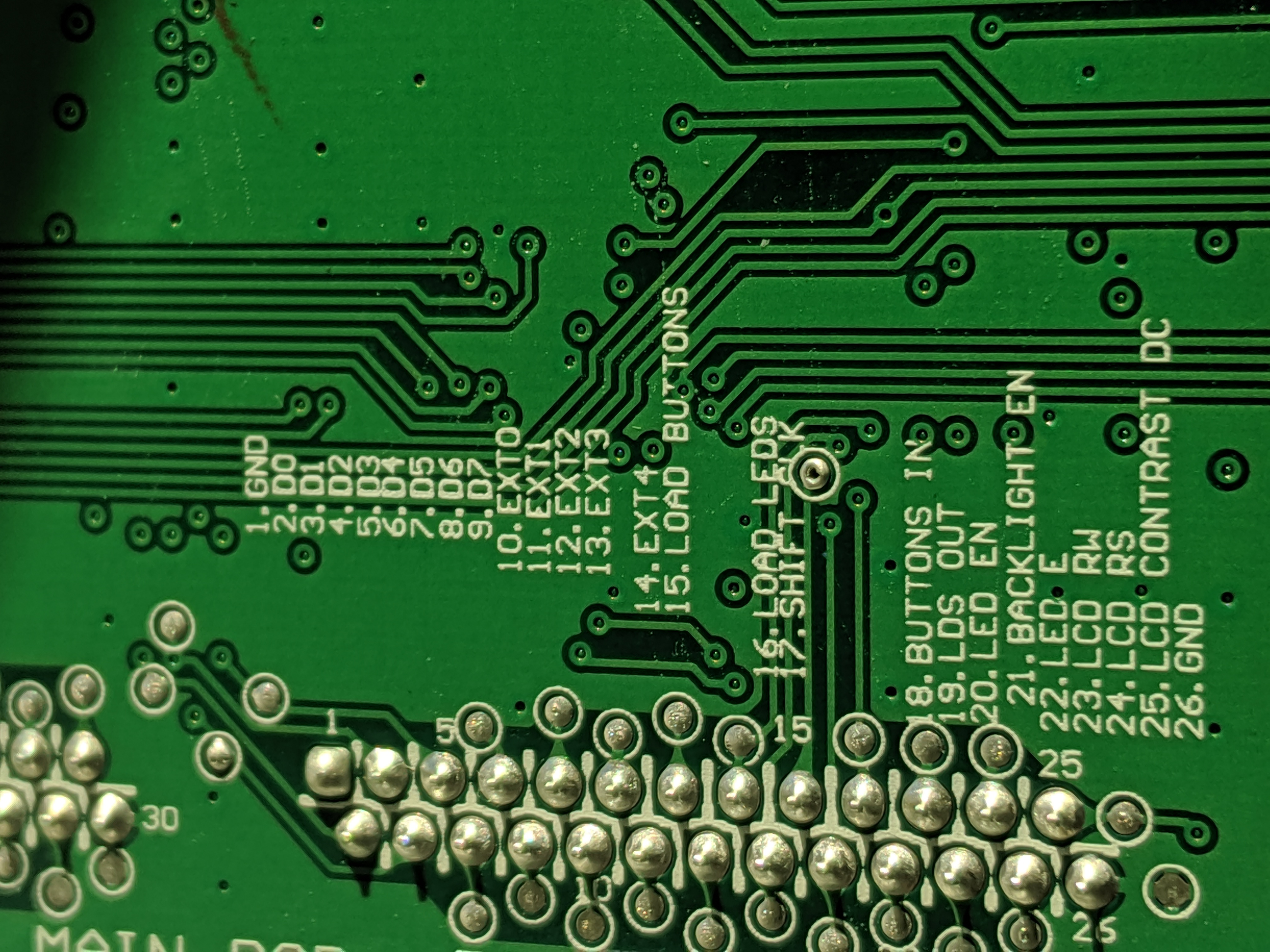
Thankfully, we can learn a lot from the text, and it matches our winstar LCD spec. Specifically, we see
- 8 pins [D0-D7] for data
- LCD RW
- LCD RS
- LCD E(nable) and
- LCD Contrast DC (which appears to be the voltage potentiometer to alter the screen contrast).
and some other stuff that doesn’t belong, like “Load LEDS”. So this pinout is probably doing double duty.
Now, the trick is to figure out which GPIO pins are mapped to which of the labelled outlets on the PCB.
So we set some breakpoints in GDB when characters are being written to the screen and hopefully we can figure out what’s going on.
Go understand how GPIO works before you read further.
STM32F103 memory-maps its perpherials. Which means everything, clocks, output voltages driving LCDs, USB,
is just another address.
Here’s a handy cheatsheet on how GPIO works.
Every GPIO ‘port’ (a-e) has 16 pins it drives, which are physical pieces of metal sticking out of the CPU
which are wired via ribbon cable to the MPK2 device.
Mostly, the pins are written via the 0x10 address extension (BSRR).
Critically, you need to watch (and set) two seperate things, the GPIO configuration (is the pin input or output, what is its speed etc)., and the data coming out of the pin (0 or 1).
The below 4 gdb instructions will show you config status (0x00) and data read (0x08) address values for GPIOB and GPIOC.
Theoretically, if just GPIOB and GPIOC are driving the LCD, these four values are all we need to track over time to
see how the LCD is being driven. Ideally, it will map to the ST7066 spec sheet linked above, and not some
random nonsense reflecting hidden knowledge we can’t obtain public documentation for.
Our operating system depends on using publicly documented and non-creative, obvious mechanisms
to interface with peripherals like the screen or buttons.
display/1xw 0x40010c08
display/1xw 0x40010c00
display/1xw 0x40011008
display/1xw 0x40011000
Port B Config
Port B Data
Port C Config
Port C Data
Note also, the BSRR function just overwrites certain pin values, it
does not change them all at once. So you really need to track GPIO values over time
to understand what’s going on; it’s not enough to see a given value is stored in a GPIO register
that corresponds to BSRR, because you’re missing the current values its amending, and the port’s
current configuration.
We wrote some characters.
It appears GPIOB1 and GPIOB2 are driving the R/S and R/W bits of the LCD,
and that GPIOC0-GPIO-7 are driving the data bits. At this point this is
just a hypothesis.
0x40010c00 : 0x70000
0x40010c00 : 0x1000
0x40010c00 : 0x20000000
0x40010c00 : 0x80000000
0x40010c00 : 0x200000

0x40011008 (idr) : 0x980067
and then a g is written to the screen.
So breaking this down, what happened?
0x980067 translates to 0b100110000000000001100111, and matching
that last byte to to the ST7066 data sheet, [0110][0111] corresponds
to the letter g. So we have confirmation that GPIOC0-7 are most likely
wired to the LCD data.
Now through experiment it appears GPIOB1 and GPIOB2 are actually driving
R/S and RW. But what does GPIOB0 do? It sends the enable clock pulse
[0 - 1 - 0] to the LCD which drives one iteration of the circuit.
Don’t take my word for it, we can prove all of this is true within GDB.
Boot up an unmodified MPK249 and pause it in GDB (ctrl-z). Define a
‘clock pulse’ function.
define lcdpulse
  set {int} 0x40010c10 = 0x1
  shell sleep .1
  set {int} 0x40010c10 = 0x10000
end
where this is proven to work on Mac and LINUX, but the ‘shell sleep .1’ needs an equivalent
Windows command. Isn’t this cool? We can use GDB to test out certain ideas and write
fragments of code to verify those ideas before we even code them.
While the debugger is paused, make sure the lower 8 GPIOC pins are set to write
set {int} 0x40011000 = 0x33333333
Write in the character ‘g’ into the LCD data:
set {int} 0x40011010 = 0x980067
and then
Wow! ‘g’ has been written to the screen.
A small matter of contrast
At this point, we have everything we need to write a quick driver in C
to drive the LCD. Except hmm. We know a potentiometer is supposed to change the
LCD contrast, and it’s not exactly apparent how this digital chip can
send precisely tuned voltage. And which pin is doing it?
By experimenting with all the GPIO pins, we can figure it out.
Watch the GPIOB configuration and data.
display/1xw 0x40010c08
display/1xw 0x40010c00
Ok, this is weird. If we pause the debugger and just stepi through the instructions, we notice
x/xw 0x40010c08 0x40010c08: 0x0000ffd4
x/xw 0x40010c08 0x40010c08: 0x0000fff4
and back and forth. It looks like pin B5 is flipping back and forth between 1 and 0 on its own.
Learning about pulse width modulation here: link. This seems like an interesting candidate.
And look at Pin 5’s configuration.
(gdb) x 0x40010c00
0x40010c00:	0x44b84222
What the heck does b mean? ‘Alternative function?’ That seems new. If we set that pin to read
set {int} 0x40010c00 = 0x44484222
the screen contrast goes to 0. Ok. And if we change it from b to write:
set {int} 0x40010c00 = 0x44184222
the screen goes full contrast. Ok we’re getting somewhere.
Shortcutting through pulse width modulation and timers.
So Pin B5 is flickering alot, by itself apparently. And its voltage
seems to drive the potentiometer, somehow. We also see its configuration
is in this new ‘alternative function’. What is that?
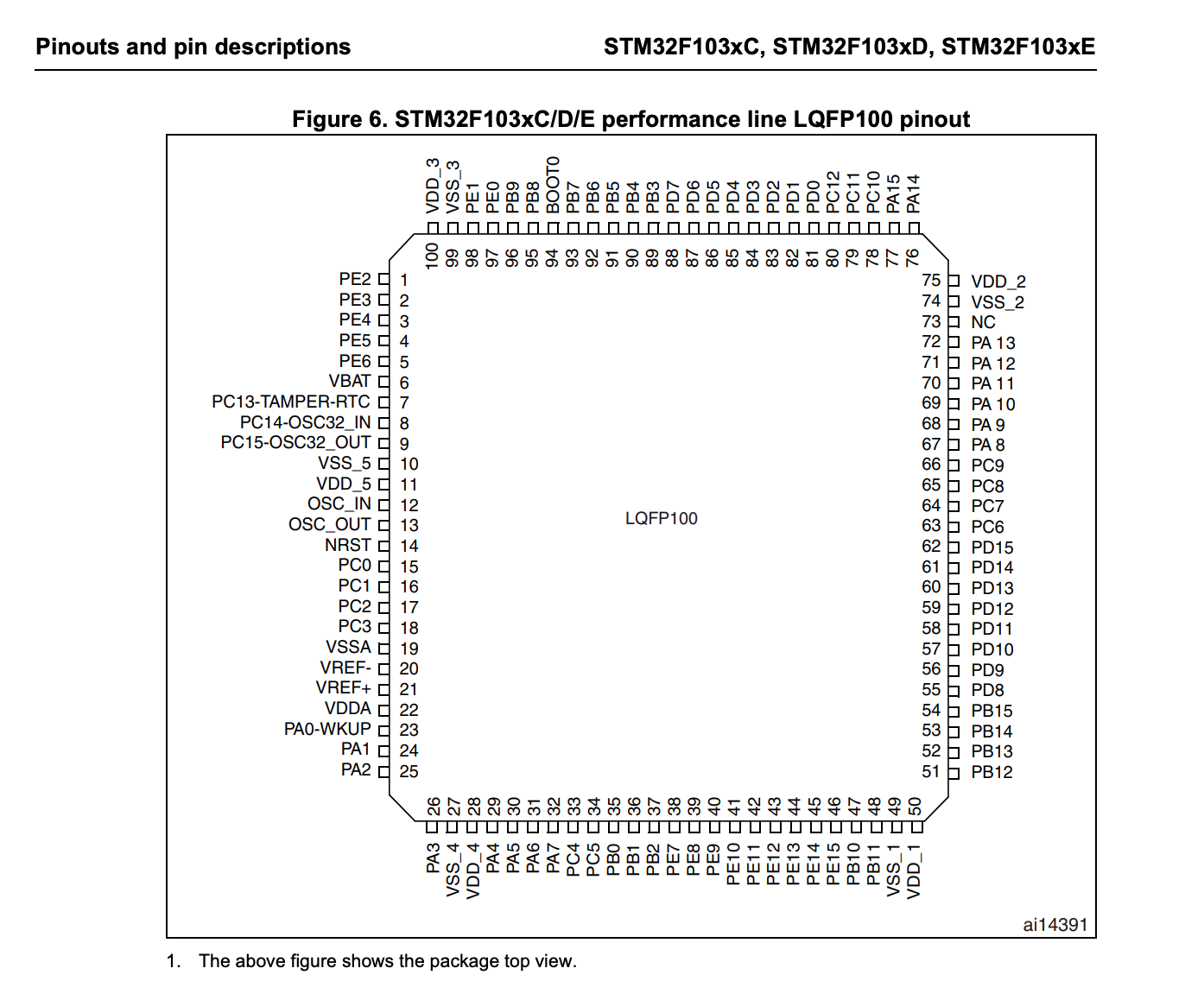
There’s a pin diagram for our chip, a high density, LQFP, 100 pin STM32F103 C series.
We see from the spec sheet that PIN B5 corresponds to TIM3, which is a clock ticky peripheral.
At this point, we could go learn about that, but let’s see how much we can get away with just
by reading TIM3 values in gdb! It’s a memory-mapped peripheral system after all, and there should
be no hidden variables. If TIM3 does stuff, let’s see if we can learn just by watching it.
Cool. So boot up the stock OS and go into the Contrast change mode.
Let’s spy on TIM3
When we start with the contrast value at 50
Contrast 50:
TIM3
                    0                 4              8               c
0x40000400:	0x00000081	0x00000000	0x00000000	0x00000000
0x40000410:	0x0000001f	0x00000000	0x00006800	0x00000000
0x40000420:	0x00000010	[0x00000141]	0x00000000	0x000001df
0x40000430:	0x00000000	0x00000000	0x00000155	0x00000000
0x40000440:	0x00000000	0x00000000	0x00000000	0x00000081
where [] seems to go up and down as we stepi,
no matter what else is happening in the system.
Contrast 99:
TIM3
0x40000400:	0x00000081	0x00000000	0x00000000	0x00000000
0x40000410:	0x0000001f	0x00000000	0x00006800	0x00000000
0x40000420:	0x00000010	[0x000000df]	0x00000000	0x000001df
0x40000430:	0x00000000	0x00000000	<0x000001de>	0x00000000
0x40000440:	0x00000000	0x00000000	0x00000000	0x00000081
Where [] keep changing, and <> seems permanently changed, and associated
with the changed contrast.
Contrast 00: makes that <> value = 0x000000c8, but everything else behaves the same.
Ok interesting. So some values are set in TIM3, one value seems to change directly
with when we spin the contrast knob, and one value just ticks up and down in a circle
regardless of what we do. Let’s go check the address maps in Ghidra and see if we can make sense of
it.
Consulting the SVD file, w.r.t. TIM3 ->
40000400 = CR1, this is set to 0x81
40000410 = SR , this is set to 0x1f
40000418 = CCMR_Input1, this is set to 0x00006800
40000420 = CCER, this is set to 0x10
40000424 = CNTR (counter), this is going all over the place, even during debug mode. Not sure we set it.
40000428 = Prescaler. Not set to anything. But we note it because it's mentioned alot in PWM docs.
4000042c = ARR, this is set to 0x000001df
40000438 = CCR2, this is what seems to go between 0x000000c8 - 0x000001de, with 0x155 the center.
CCR2 the configurable parameter.
Cool, just by watching and skipping learning absolutely everything about pulse width modulation,
we have learned 95% of what it takes to drive the contrast. In fact, this is our basic contrast function in the operating system!
We skips tons of HALs and system libraries and confusion, and just cut straight to the heart of the matter.
void contrast(){
  TIM3 -> CR1 = 0x81;
  TIM3 -> SR  = 0x1f;
  TIM3 -> CCMR1 = 0x00006800;
  TIM3 -> CCER = 0x10;
  TIM3 -> ARR  = 0x000001df;
  TIM3 -> CCR2 = 0x00000155; // This is the contrast value.
  TIM3 -> DMAR = 0x00000081;
}
7 lines is cool.
When you boot up an operating system with that function called, things seem pretty good.
Our TIM3 values look just like the TIM3 values in the stock operating system, except
Pin B5 is not flickering the way we’d expect. Contrast is 0. How do we hook TIM3
to Pin B5?
A little internet investigation reveals
    RCC_APB1PeriphClockCmd(RCC_APB1Periph_TIM3, ENABLE);
    RCC_APB2PeriphClockCmd(RCC_APB2Periph_AFIO, ENABLE);
    GPIO_PinRemapConfig(GPIO_PartialRemap_TIM3, ENABLE);
That plus our contrast function, we’re in business! We now have all the ingredients to write a full LCD driver.
Now, we skipped past a lot of learning and understanding by just watching the TIM3 values and trying to clone them.
Let’s spend a moment understanding what just happened. We set 7 pointers in TIM3
CR1, SR, CCMR1, CCER, ARR, CCR2, and DMAR.
Let’s consult Page 35 of the STM32 Timer Cookbook).